Applied Materials Unveils Chip Wiring Innovations for More Energy-Efficient Computing
Applied Materials Unveils Chip Wiring Innovations for More Energy-Efficient Computing
- Industry's first use of ruthenium in high-volume production enables copper chip wiring to be scaled to the 2nm node and beyond and reduces resistance by as much as 25%
- New enhanced low-k dielectric material reduces chip capacitance and strengthens logic and DRAM chips for 3D stacking
- 业界首次使用钌在高容量生产中,使铜芯片布线能够扩展到2纳米节点及更高,并将电阻降低高达25%。
- 新增强低介电材料可减少芯片电容和加强逻辑和DRAM芯片的三维堆叠
SANTA CLARA, Calif., July 08, 2024 (GLOBE NEWSWIRE) -- Applied Materials, Inc. today introduced materials engineering innovations designed to increase the performance-per-watt of computer systems by enabling copper wiring to scale to the 2nm logic node and beyond.
美国加利福尼亚州圣塔克拉拉,2024年7月8日(环球社交媒体公司)- 应用材料公司今天推出了材料工程创新,旨在通过使铜线缩放到2纳米逻辑节点及更高,从而提高计算机系统的性能 - 每瓦功率。
"The AI era needs more energy-efficient computing, and chip wiring and stacking are critical to performance and power consumption," said Dr. Prabu Raja, President of the Semiconductor Products Group at Applied Materials. "Applied's newest integrated materials solution enables the industry to scale low-resistance copper wiring to the emerging angstrom nodes, while our latest low-k dielectric material simultaneously reduces capacitance and strengthens chips to take 3D stacking to new heights."
“AI 时代需要更节能的计算,而芯片布线和堆叠对性能和能耗至关重要,”应用材料半导体产品组总裁Dr. Prabu Raja表示:“应用的最新集成材料解决方案使行业能够将低电阻铜线扩展到新兴的阿兹特克节点,而我们最新的低介电材料则可同时减少电容并增强芯片,将3D堆叠推向新的高度。”
Overcoming the Physics Challenges of Classic Moore's Law Scaling
克服传统摩尔定律缩放的物理挑战
Today's most advanced logic chips can contain tens of billions of transistors connected by more than 60 miles of microscopic copper wiring. Each layer of a chip's wiring begins with a thin film of dielectric material, which is etched to create channels that are filled with copper. Low-k dielectrics and copper have been the industry's workhorse wiring combination for decades, allowing chipmakers to deliver improvements in scaling, performance and power-efficiency with each generation.
如今,最先进的逻辑芯片可以包含数百亿个晶体管,这些晶体管通过60英里以上的微小铜线相连接。芯片每一层的布线都始于薄膜介电材料,该材料被刻蚀以创建通道,这些通道被填充有铜。低k介电材料和铜是行业的支柱布线组合数十年,使芯片制造商能够在每一代中提供缩放、性能和功率效率的改进。
However, as the industry scales to 2nm and below, thinner dielectric material renders chips mechanically weaker, and narrowing the copper wires creates steep increases in electrical resistance that can reduce chip performance and increase power consumption.
然而,随着行业缩放到2纳米及以下,更薄的介电材料使芯片在力学上更加脆弱,而缩小铜线会导致电阻急剧增加,这可能会降低芯片性能并增加能耗。
Enhanced Low-k Dielectric Reduces Interconnect Resistance and Strengthens Chips for 3D Stacking
增强的低介电材料可减少互连电阻并加强三维堆叠芯片
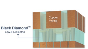
Applied's Black Diamond material has led the industry for decades, surrounding copper wires with a low-dielectric-constant – or "k-value" – film engineered to reduce the buildup of electrical charges that increase power consumption and cause interference between electrical signals.
多年来,Applied的黑钻石材料一直领导着行业,在铜线周围进行低介电常数-或“k值”-薄膜的包围,该薄膜被设计用于减少电荷的积聚,从而增加功耗并在电信号之间造成干扰。
Applied today introduced an enhanced version of Black Diamond, the latest in the company's Producer Black Diamond PECVD* family. This new material reduces the minimum k-value to enable scaling to 2nm and below, while offering increased mechanical strength which is becoming critical as chipmakers and systems companies take 3D logic and memory stacking to new heights.
Applied今天推出了Black Diamond的增强版本,这是公司黑钻石生产线的最新产品。这种新材料可降低最小k值,使其可扩展到2纳米及以下,并提供了越来越关键的机械强度,因为芯片制造商和系统公司将三维逻辑和存储堆叠推向新的高度。
The latest Black Diamond technology is being adopted by all leading logic and DRAM chipmakers.
领先的逻辑和DRAm芯片制造商正在采用最新的Black Diamond技术。
New Binary Metal Liner Enables Ultrathin Copper Wires
新的二元金属衬底可实现特薄铜导线
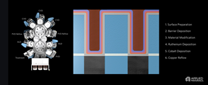
To scale chip wiring, chipmakers etch each layer of low-k film to create trenches, then deposit a barrier layer that prevents copper from migrating into the chip and creating yield issues. The barrier is then coated with a liner that ensures adhesion during the final copper reflow deposition sequence, which slowly fills the remaining volume with copper.
为了扩展芯片布线,芯片制造商会刻蚀低k膜的每一层以创建沟槽,然后涂一层屏障层,以防铜迁移到芯片中并造成产量问题。然后在屏障上涂覆一层衬底,以确保在最终的铜再流入沉积序列期间具有黏附性,该序列慢慢用铜填充剩余体积。
As chipmakers further scale the wiring, the barrier and liner take up a larger percentage of the volume intended for wiring, and it becomes physically impossible to create low-resistance, void-free copper wiring in the remaining space.
随着芯片制造商进一步缩放布线,屏障和衬底占用了剩余空间的较大比例,无法在剩余空间中创建低电阻的无瑕铜导线,这在物理上变得不可能。
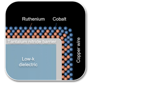
Today, Applied Materials publicly introduced its latest IMS (Integrated Materials Solution) which combines six different technologies in one high-vacuum system, including an industry-first combination of materials that enables chipmakers to scale copper wiring to the 2nm node and beyond. The solution is a binary metal combination of ruthenium and cobalt (RuCo), which simultaneously reduces the thickness of the liner by 33 percent to 2nm, produces better surface properties for void-free copper reflow, and reduces electrical line resistance by up to 25 percent to improve chip performance and power consumption.
今天,Applied公开展示了其最新的IMS(集成材料解决方案),该解决方案将六种不同的技术组合在一个高真空系统中,其中包括行业首次组合的材料,使芯片制造商能够将铜线缩放到2纳米节点及更高。该解决方案是一种钌和钴(RuCo)的二元金属组合,可将衬底厚度同时降低33%至2纳米,为无瑕铜再流动提供更好的表面特性,并将电气线电阻降低了多达25%以提高芯片性能和能耗。
The new Applied Endura Copper Barrier Seed IMS with Volta Ruthenium CVD* is being adopted by all leading logic chipmakers and began shipping to customers at the 3nm node. An animation of the technology can be viewed here.
新的Applied Endura Copper Barrier Seed IMS with Volta Ruthenium CVD *的技术被所有领先的逻辑芯片制造商采用,并已开始在3nm节点向客户发货。这里可以查看技术的动画。
Customer Comments
客户评论
"While advances in patterning are driving continued device scaling, critical challenges remain in other areas including interconnect wiring resistance, capacitance and reliability," said Sunjung Kim, VP & Head of Foundry Development Team at Samsung Electronics. "To help overcome these challenges, Samsung is adopting multiple materials engineering innovations that extend the benefits of scaling to the most advanced nodes."
三星电子排Foundry开发团队副总裁Sunjung Kim表示:“虽然图案制作方面的进展推动了持续的器件缩放,但在互连线电阻、电容和可靠性等其他领域仍存在关键挑战。为了帮助克服这些挑战,三星正在采用多种材料工程创新,将缩放的好处扩展到最先进的节点。”
"The semiconductor industry must deliver dramatic improvements in energy-efficient performance to enable sustainable growth in AI computing," said Dr. Y.J. Mii, Executive Vice President and Co-Chief Operating Officer at TSMC. "New materials that reduce interconnect resistance will play an important role in the semiconductor industry, alongside other innovations to improve overall system performance and power."
台积电执行副总裁兼共同COO Dr. Y.J. Mii表示:“半导体行业必须提供能源效率性能的显著提高,以实现人工智能计算的可持续增长。减少互连电阻的新材料将在半导体行业中发挥重要作用,同时还有其他创新措施来提高整体系统性能和功率。”
A Growing Wiring Opportunity
即将到来的布线机遇
Applied is the industry leader in chip wiring process technologies. From the 7nm node to the 3nm node, interconnect wiring steps have approximately tripled, increasing Applied's served available market opportunity in wiring by more than $1 billion per 100,000 wafer starts per month (100K WSPM) of greenfield capacity, to approximately $6 billion. Looking ahead, the introduction of backside power delivery is expected to increase Applied's wiring opportunity by another $1 billion per 100K WSPM, to approximately $7 billion.
Applied是芯片连线工艺技术领域的行业领导者。从7nm节点到3nm节点,连线工艺步骤大约增加了三倍,使Applied在芯片连线方面的市场可获得机会每10万张晶圆每月(10万WSPM)的绿地产能可增加10亿美元,增加至约60亿美元。展望未来,预计背面功率传递的推出将使Applied的连线机会再增加10亿美元每10万WSPm,增至约70亿美元。
The new chip wiring products, along with other materials engineering innovations for making future AI chips, will be discussed at Applied's SEMICON West 2024 Technology Breakfast. The presentation and other materials from the event will be available on the Applied Materials website at: on Tuesday, July 9, 2024 at approximately 9:00 a.m. ET / 6:00 a.m. PT.
新的芯片连线产品以及用于制造未来人工智能芯片的其他材料工程创新技术,将在2024年Applied的SEMICON West技术早餐会上讨论。 活动的演示文稿和其他材料将在2024年7月9日星期二上午9:00 Et / 6:00 Pt左右在Applied Materials网站上提供。
*PECVD = Plasma-Enhanced Chemical Vapor Deposition
*CVD = Chemical Vapor Deposition
*PECVD = 等离子增强化学气相沉积
*CVD = 化学气相沉积
Forward-Looking Statements
This press release contains forward-looking statements, including those regarding anticipated benefits of our new products and technologies, expected growth and trends in our businesses and markets, industry outlooks and demand drivers, technology transitions, and other statements that are not historical facts. These statements and their underlying assumptions are subject to risks and uncertainties and are not guarantees of future performance. Factors that could cause actual results to differ materially from those expressed or implied by such statements include, without limitation: failure to realize anticipated benefits of our new products and technologies; the level of demand for semiconductors and for our products and technologies; customers' technology and capacity requirements; the introduction of new and innovative technologies, and the timing of technology transitions; market acceptance of existing and newly developed products; the ability to obtain and protect intellectual property rights in technologies; our ability to ensure compliance with applicable law, rules and regulations; and other risks and uncertainties described in our SEC filings, including our recent Forms 10-Q and 8-K. All forward-looking statements are based on management's current estimates, projections and assumptions, and we assume no obligation to update them.
前瞻性声明
本新闻稿包含前瞻性声明,包括有关我们新产品和技术的预期益处,我们业务和市场的预期增长和趋势,行业前景和需求驱动因素,技术转变以及其他非历史事实的声明。这些声明及其潜在假设受到风险和不确定性的影响,并不保证未来业绩。导致实际结果与此类声明所表达或暗示的结果不同的因素包括但不限于:未能实现我们新产品和技术的预期益处;对半导体和我们的产品和技术的需求水平;客户的技术和产能要求;引入新的和创新的技术以及技术转变的时机;市场对现有和新开发产品的接受程度;在技术上取得和保护技术方面的知识产权;我们确保遵守适用法律、法规和规章制度的能力;以及我们在SEC申报中描述的其他风险和不确定性,包括我们最近的10-Q和8-k表格。所有前瞻性声明都基于管理层的当前估计、投射和假设,并且我们不承担更新它们的义务。
About Applied Materials
Applied Materials, Inc. (Nasdaq: AMAT) is the leader in materials engineering solutions used to produce virtually every new chip and advanced display in the world. Our expertise in modifying materials at atomic levels and on an industrial scale enables customers to transform possibilities into reality. At Applied Materials, our innovations make possible a better future. Learn more at .
关于应用材料
应用材料公司(纳斯达克:AMAT)是世界上几乎所有新芯片和先进显示技术的材料工程解决方案的领导者。我们的专业知识使客户能够将材料在原子层面和工业规模上进行改性,从而将可能转化为现实。在应用材料公司,我们的创新使更美好的未来成为可能。了解更多信息。
Applied Materials Contact:
Ricky Gradwohl (editorial/media) 408.235.4676
Michael Sullivan (financial community) 408.986.7977
应用材料联系人:
Ricky Gradwohl(编辑/媒体)408.235.4676
Michael Sullivan(金融界)408.986.7977
Photos accompanying this announcement are available at
附带的照片可在以下网址获取

Applied Materials' Latest Integrated Materials Solution Extends Copper Wiring to 2nm and Beyond
应用材料的最新集成材料解决方案将铜线延伸到2纳米及以上

Applied Materials' new Endura Copper Barrier Seed IMS with Volta Ruthenium CVD combines six different technologies in one high-vacuum system, including an industry-first combination of materials that enables chipmakers to scale copper wiring to the 2nm node and beyond.
应用材料的新Endura Copper Barrier Seed IMS与Volta Ruthenium CVD在一个高真空系统中结合了六种不同的技术,包括行业首次组合的材料,使芯片制造商能够将铜线缩放到2纳米及以上。
Combining Ruthenium and Cobalt Improves Chip Performance and Power Consumption
组合钌和钴可以提高芯片性能和降低功耗

With the semiconductor industry's first use of ruthenium in high-volume production, Applied Materials' new binary metal combination of ruthenium and cobalt (RuCo) enables copper chip wiring to be scaled to the 2nm node and beyond and reduces electrical line resistance by as much as 25 percent.
在半导体行业首次使用钌进行高产量生产,应用材料的新二元金属组合钌和钴(RuCo)使得铜芯片线缩放到2纳米及以上,并将电器线电阻降低高达25%。
Enhanced Black Diamond Reduces Interconnect Resistance and Strengthens Chips for 3D Stacking
增强型黑色金刚石可以减小互连电阻并强化3D堆叠芯片

Applied Materials today introduced an enhanced version of the company's Producer Black Diamond PECVD dielectric film. This new material enables chip scaling to 2nm and below, while offering increased mechanical strength to help take 3D logic and memory stacking to new heights.
应用材料今天推出了公司的Producer Black Diamond PECVD介电薄膜的升级版。这种新材料可以在提供更大机械强度的同时,将芯片缩放到2纳米及以下,以促进3D逻辑和内存堆叠技术的发展。
Source: Applied Materials, Inc.
资料来源:应用材料公司
