ASML and Imec Open Joint High NA EUV Lithography Lab Offering an Early Development Platform to the Leading-edge Semiconductor Ecosystem
ASML and Imec Open Joint High NA EUV Lithography Lab Offering an Early Development Platform to the Leading-edge Semiconductor Ecosystem
Imec, a world-leading research and innovation hub in nanoelectronics and digital technologies, and ASML Holding N.V. (ASML), a leading lithography supplier to the semiconductor industry, have announced the opening of the High NA EUV Lithography Lab in Veldhoven, the Netherlands, a lab jointly run by ASML and imec. After a build and integration period of years, the Lab is ready to provide leading-edge logic and memory chip makers, as well as advanced materials and equipment suppliers access to the first prototype High NA EUV scanner (TWINSCAN EXE:5000) and surrounding processing and metrology tools.
愛文思控股(ASML Holding N.V.)與全球領先的納米電子和數字技術研究和創新中心Imec宣佈在荷蘭菲爾德霍芬開設高NA EUV光刻實驗室,這是由ASML和Imec合作運營的實驗室。經過多年的建設和集成,實驗室已準備好提供最先進的邏輯和存儲芯片製造商以及先進材料和設備供應商使用首臺原型高NA EUV掃描儀(TWINSCAN EXE:5000)和周圍的處理和計量工具。
The opening of the joint ASML-imec High NA EUV Lab represents a milestone in preparing High NA EUV for high-volume manufacturing – anticipated to happen in the 2025–2026 timeframe. By giving leading-edge logic and memory chip manufacturers access to the High NA EUV prototype scanner and surrounding tools (which include a coat and development track, metrology tools, wafer and mask handling systems), imec and ASML support them in de-risking the technology and develop private High NA EUV use cases before the scanners will be operational in their production fabs. Access will also be provided to the broader ecosystem of material and equipment suppliers and to imec's High NA patterning program.
ASML-Imec聯合開設的高NA EUV實驗室在利用高NA EUV進行大規模製造方面邁出了重要一步,預計會在2025-2026年實現。Imec和ASML通過使領先的邏輯和內存芯片製造商可以使用高NA EUV原型掃描儀及其周圍的工具(其中包括塗覆和開發系統、計量工具、晶片和掩膜處理系統),支持他們在掃描儀開始運行於他們的生產工廠之前,降低技術風險、開發私有的高NA EUV應用案例。同時,高NA EUV實驗室也將爲材料和設備供應商以及Imec的高NA圖案計劃提供支持。
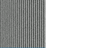
Readying the 0.55 NA EUV scanner and infrastructure followed intense preparations that started in 2018. In this time span, ASML and ZEISS were able to develop High NA EUV scanner specific solutions related to the source, optics, lens anamorphicity, stitching, reduced depth of focus, edge placement errors and overlay accuracy. Meanwhile, imec, in tight collaboration with its extended supplier network, prepared the patterning ecosystem, including the development of advanced resist and underlayer materials, photomasks, metrology and inspection techniques, (anamorphic) imaging strategies, optical proximity correction (OPC), and integrated patterning and etch techniques. The preparatory work recently resulted in first exposures, showing for the first time ever 10 nm dense lines (20 nm pitch) printed in Veldhoven on metal oxide resists (MORs) using the 0.55 NA EUV prototype scanner.
準備0.55 NA EUV掃描儀和基礎設施的工作始於2018年。在這個時間段內,ASML和ZEISS能夠開發出與源、光學、透鏡非等軸性、拼接、減小的焦深、邊緣放置誤差和覆蓋精度有關的高NA EUV掃描儀特定解決方案。與此同時,Imec與其擴展的供應商網絡緊密合作,準備了圖案生態系統,包括開發先進的抗蝕劑和底層材料、光掩膜、計量和檢驗技術、(非等軸性)成像策略、光學鄰近效應校正(OPC)以及集成圖案和刻蝕技術。這項準備工作最近產生了第一次曝光,首次在荷蘭菲爾德霍芬使用0.55 NA EUV原型掃描儀在金屬氧化物抗蝕劑上印刷了10納米的密集線(20納米間距)。
Imec's president and CEO Luc Van den hove: "High NA EUV is the next milestone in optical lithography, promising the patterning of metal lines/spaces with 20 nm pitch in one single exposure and enabling next generations of DRAM chips. This will improve yield and reduce cycle time and even CO2 emissions compared to existing multi-patterning 0.33 NA EUV schemes. It will therefore be a key enabler to push Moore's Law well into the ångström era. We are now thrilled to explore these capabilities in real life, using the prototype High NA EUV scanner. For imec and its partners, the High NA EUV Lithography Lab will act as a virtual extension of our 300 mm cleanroom in Leuven, enabling us to further improve the patterning ecosystem and push the resolution of the High NA EUV towards its ultimate limits."
Imec的總裁兼首席執行官Luc Van den Hove:"高NA EUV是光刻技術的下一個里程碑,可以在一次曝光中實現20納米間距的金屬線/空間圖案,並且可以實現下一代DRAM芯片。這將提高產量、降低週期時間,甚至比現有的多模式0.33 NA EUV方案更少產生CO2排放。因此,它將是將摩爾定律推向埃普斯特朗時代的關鍵推動因素。現在我們非常激動地使用這臺原型高NA EUV掃描儀探索這些能力。對於Imec及其合作伙伴而言,高NA EUV光刻實驗室將作爲其勒芬300mm晶圓廠的虛擬擴展,使我們能夠進一步改進圖案生態系統,並將高NA EUV的分辨率推向其極限。"

