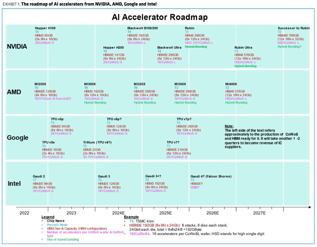
Bernstein believes that with the accelerated iteration of AI chips, Nvidia's leading edge over other manufacturers will expand further, TSMC's advanced packaging advantage is expected to continue, and the ASIC chip market is expected to expand.
Author of this article: Li Xiaoyin
Source: Hard AI
Overnight in the US stock market, semiconductor giant TSMC had a market capitalization of 1 billion US dollars. Taiwanese stock prices also hit a record high on Monday, indicating that the market's demand for high-end chips, especially AI chips, is still strong.
On July 8, investment bank Bernstein analysts Mark Li, Stacy A. Rasgon and others released a research report summarizing the AI chip technology transformation roadmap to 2027, analyzing the four fields of design architecture, wafer nodes, HBM, and advanced packaging, and discussing their possible impact.
AI chips accelerate iteration, Nvidia may become the biggest winner

Bernstein believes AI chips will accelerate development, and Nvidia in particular has accelerated the iteration rate to “one change a year.”
Technology Roadmap 1 shows Nvidia's dramatic changes from Blackwell to Rubin, including all changes in the architecture, nodes, HBM, and package in about 1 year — nodes from N4 to N3, HBM from 3E to 4, and package sizes from smaller (a single CoWOS wafer holds 16 B100/B200) to larger (a single CoOS wafer holds up to 10 Rubin).
Additionally, the Nvidia HBM upgrade update from 8Hi/192GB to 12Hi/288GB will be completed within 6 months.
In contrast, AMD's pace is slightly slower: the MI325X was launched about a year later than the MI300X and will only upgrade the memory; by 2025, the MI350X will mainly upgrade to N3 nodes, but the memory and capacity will remain the same, and will still be the HBM3E 288GB.
According to the report, this will have the first impact: as AI chips accelerate iteration, Nvidia's leading edge over other vendors will expand further.


The second impact is the trend of CPU and GPU integration, memory and logic integration. For example, Nvidia integrated the CPU and GPU into its GB200 to help its Arm-based CPUs take advantage of the leading edge in the GPU field.
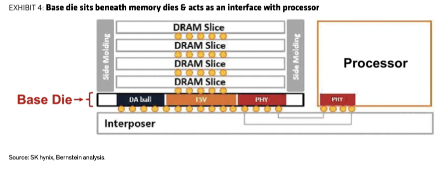
Technology Roadmap 3 shows that in order to further promote the development of data transmission, HBM4 may begin to provide customer customization services based on basic chips. Since customization of its basic die (logic die) requires a longer production cycle, integration of logic and storage within HBM may become a major trend.

TSMC's advanced packaging advantages are expected to continue
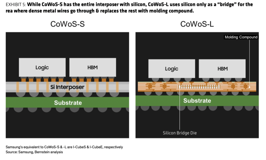
The report points out that TSMC's technical advantages will continue, growing from CoWoS-S to Cowos-L.
According to reports, the entire middleware of CoWoS-S uses silicon, while CoWoS-L only uses silicon as a “bridge” in the area where dense metal wires pass through, and the rest is replaced with molding compounds.

The report predicts that in the future, almost all AI chips will be packaged using TSMC's CowOS, and it is expected that customers will expand to Microsoft (partly through Marvell) and Meta (via Broadcom) in the next step. This will also have a third major impact: as technology continues to advance and the customer base continues to expand, TSMC's leading position in advanced packaging will continue, if not to expand.
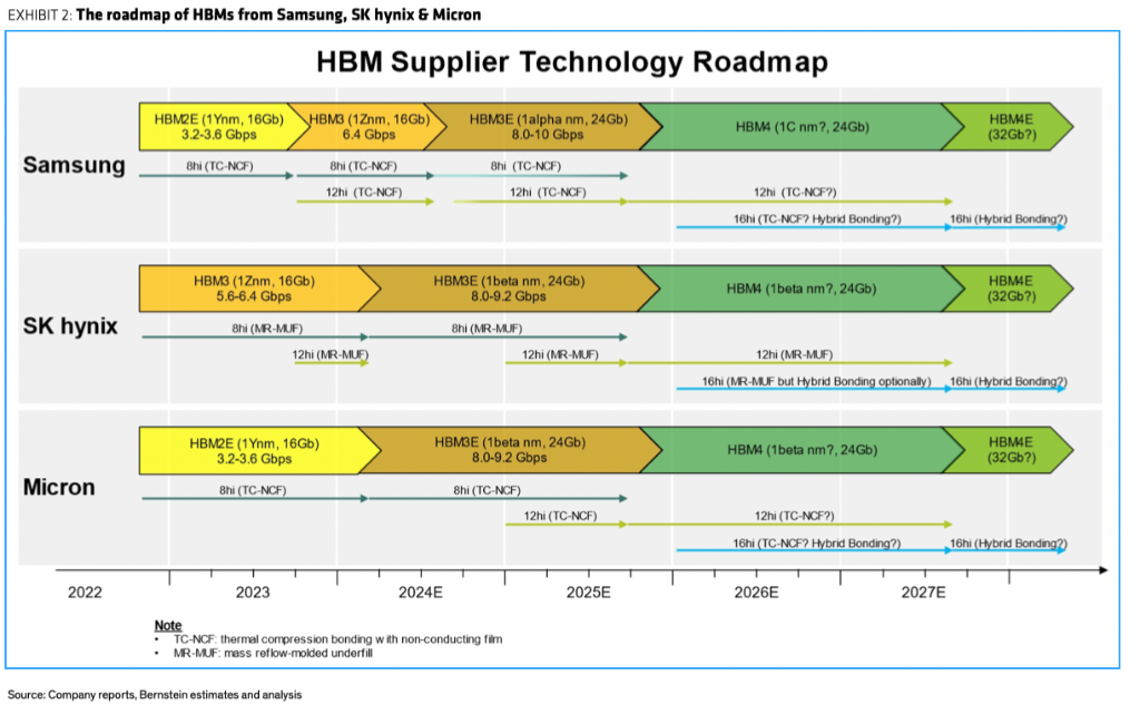
Fourth, I hope Samsung can keep up with HBM3E in time. Currently, Samsung has not announced its HBM3E certification, specifically from Nvidia.
According to the report, although Samsung started late in HBM3E, the HBM3E window will still provide Samsung with an opportunity to catch up. Almost all Nvidia chips in 2025 and chips from other manufacturers in 2026 are likely to still use HBM3E.
The outlook for demand for bonding technology is optimistic, and the ASIC market is expanding
As the node transition continues, the report predicts that AI will make N2 a “supernode,” but this underestimates production and cost burdens — advanced packaging awards become more difficult as the level expands — making bonding technology, particularly hybrid bonding technology, critical in vertical stacking.
Bernstein is structurally optimistic about the long-term future of bonding technology. The report argues that the fifth impact is that AI chips and other related applications (wafer-to-wafer, chip-to-wafer, or chip-to-chip) will bring a larger market for bonding technology.
Sixth, panel level packages (PLP) can scale horizontally more than wafer-level packages because the former can guarantee a better level of scalability, but this transformation requires effort and may take longer than expected.
According to the report, Samsung owns wafers and panels and is trying to create a leading edge through PLP, which should have an advantage over Intel and TSMC in this regard.
Finally, for ASIC chip providers, the surge in AI chips will attract new entrants while also greatly expanding the market.
According to the report, attracted by market growth, many companies are entering the field of ASIC (High Performance Specific Integrated Circuit) chips. Because of their simpler hardware specifications and advantages in terms of work efficiency and cost, they are seen as viable alternatives to GPUs. Tech giants including Amazon, Microsoft, and Meta are developing ASIC chips.
However, since the target audience of ASIC chips is mostly internet companies or companies that have not had much experience in the past, they need help from ASIC service providers to develop custom chips.
According to the report, Broadcom is clearly in a leading position in this field, with revenue reaching billions of dollars. Customers include Google, Meta, etc. In addition, MediaTek also has certain competitiveness due to its strong technical capabilities in SerDes IP and advanced node packaging.
